
Differential Probe Probing Some Differences
Introduction
! Please note, documentation is still in progress !
This project was an ultra high input impedance (0.5pF||30MΩ or better) high bandwidth differential oscilloscope probe designed, built, and revised over the course of two weekends for the 2014 MakeMIT hardware hackathon. It can be built for about $30 in parts, plus the cost of etching or sending out a PCB and (optionally) 3D printing a chassis. A list of downloads necessary to build a complete probe is available at the bottom of this page. The project was in the top 10 the first week, advancing the team to the second week, where it took second place.
The objective of the project was to provide hobbyists with an affordable means to make high speed measurements, in which respect I would call it a great success. I was able to use the probe to measure various data converter waveforms from my digital oscilloscope project that I had otherwise been unable to get good data on. For example, here is a 100MHz ADC clock waveform:

And the LSB:

These measurements aren’t perfect, but they do provide a reasonable estimate of signal integrity (ie. is the signal loaded down? is it passably square?), which is very useful for debugging.
Sadly, due to the limited time and materials available, we were unable to achieve the 1GHz bandwidth that we designed for, instead we reached about 300MHz. The reasons for this are discussed towards the end of the write-up.
My team consisted of 5 students including myself. I was responsible for the electrical design and fabrication, while my teammates worked on designing a 3D printed chassis for the probe, documented our progress, and helped with board etching and assembly. The timestamps in my writeup are approximate and only tell the story from my perspective, a lot more was going on at the same time!
Week 1 (February 15, 2014):
9:30 AM – 11:30 AM: Design and Simulation
The first order of business was to pick a topology and get it working in a SPICE simulation. Because Texas Instruments was kind enough to overnight free samples of a number of different high speed opamps, I decided to use TINA-TI, which is a free graphical front end for SPICE distributed by TI that includes built-in models for all of TI’s linear ICs. We were not supposed to do any design before the hackathon other than figuring out what non-standard parts we should bring. Therefore, a few days before the hackathon, I simply picked three different high speed opamps from TI that looked good, the THS3201, THS3202, and LMH6702, verified that their models looked OK in TINA-TI, and waited until the day of to decide which one to use and how to hook it up.
The first thing that becomes apparent when thinking about designing the differential amplifier is that a single opamp configured as a differential amplifier doesn’t make for a very good probe because there is a tradeoff between bandwidth and input impedance. The larger you make the gain-setting resistors, the higher the input impedance, but the feedback path is slowed down because the pole created by the feedback resistance and opamp input capacitance moves to the right when the feedback resistance is increased. To put that in more human terms, the feedback resistance and input capacitance form a lowpass filter, which slows down the opamp. Because we desire an extremely high input impedance, a single opamp is impractical. What can we do?
The textbook solution to the input impedance issue is to add an opamp buffer to each differential input channel, thus allowing the differential stage to have a low input impedance, which is seen by the high input impedance buffers instead of the input signal. This is the circuit you will mostly likely find if you search for “opamp differential amplifier”. Unfortunately, at high frequencies, we would really prefer not to use opamps where we don’t have to. Not only are high frequency opamps relatively expensive, incentivising us to use them sparingly, but the use of feedback also introduces stability issues.

Vanilla-Flavored Differential Amplifier Schematic
In a high speed application, it is a poor choice to connect the output of an opamp directly to one of its inputs (as seen in a standard buffer circuit) because the input capacitance of the opamp will be driven directly by the output, reducing the phase margin and potentially resulting in oscillations. If you’re unfamiliar with those terms, the intuitive way to understand why this is a problem is to think about the phase shift introduced by the input capacitance of the opamp at high frequencies. This phase shift adds to the phase shift internal to the opamp (ideally an opamp transfer function will look approximately like a first order lowpass, with an extremely high DC gain) and the closer the overall phase shift at the maximum unity gain frequency is to -180 degrees, the closer the system is to a positive feedback oscillator, and the greater tendency it will have to overshoot and ring. The solution is to add a resistance into the feedback path, which tames the opamp’s output, but also slows it down. I tried this approach first, but was unable to simulate a buffered differential amplifier with satisfactory bandwidth (the target was 1GHz), so I moved on to a different approach, using a pair of MOSFET source followers without feedback as input buffers.
The best part of the source follower approach is that someone else had already designed a single-ended scope probe circuit with excellent bandwidth: the article was in a 2004 release of the Elektor magazine. I had also ordered several high speed MOSFETs and BJTs from Digikey before the hackathon, among which were several of the BF998 devices required to build the Elektor circuit (this was not an accident!). If I had more time, I would have liked to modify the design to include current source biasing of the MOSFETs to a negative supply rail in order to increase the input range and improve the linearity of the buffers. Realistically, however, this would add too much extra risk to a project that needed to be completed in only a day.
Here’s the Elektor circuit in LTSpice (because it appears TINA-TI can’t perform temperature sweeps). Note that I added a 200 ohm resistor in series with the input capacitor because it was resonating with the gate’s parasitic inductance, a 30 meg input resistor to boost the low frequency response, and a 2pF capacitor in parallel with the source resistor to squash a bump in the high frequency response.

Input Buffer Schematic
And here’s a Bode plot of the frequency response at 15, 25, and 35 degrees Celsius. There is some variation (about 0.2dB, or 1%, per 10 degrees C) in gain that might not be acceptable for a commercial grade probe, but adding temperature compensation would likely involve biasing the BF998 with some sort of PTAT current source, which was not feasible in the timeframe of the project.

Input Buffer Frequency Response at 15, 25, and 35 Degrees C
As you might notice from the Bode plot, an added advantage of the Elektor circuit is that is adds a 10x (20dB) attenuation, which means the differential amplifier sees low signal amplitudes and we can safely ignore “large signal” effects such as slew rate limiting. It’s also convenient as it increases the (likely limited) input range of whatever high speed scope we use. For example, the sampling heads on my Tektronix CSA803 scope have a maximum non-destructive input range of ±3V, which is unsuitable for scoping common 5V logic level signals. The final schematic of the probe’s amplifier circuitry in TINA-TI is shown below.

Schematic of the Analog Section
And here is a Bode plot of the differential input mode frequency response. The bandwidth looks pretty good! The phase response leaves something to be desired, but I considered it to be acceptable for the purposes of this project.

Differential Mode Bode Plot
I didn’t simulate the common mode response because the CMRR of the opamp is extremely high; the limitation to the CMRR in this circuit is due to gain mismatch between the two input buffers, which results from mismatch between the passive components in the signal path. This is not something that TINA-TI can simulate well because the tolerances on the components don’t necessarily reflect the maximum deviation we expect to see. Realistically, if two resistors or capacitors are part of the same batch of components and are next to each other on the same reel, then they will tend to be matched very well to each other, although their accuracy with respect to their rated value is still dictated by their tolerance.
Because we want the probe to be easy to use, the +5V and -5V power supplies need to be derived from a commonly-available power source. The most annoying “feature” of commercial active probes are the proprietary power connectors they integrate onto the BNC connector. What’s worse is that the design and pinouts of these connectors are poorly documented and change between generations of scopes from the same manufacturer (oh, and of course they’re incompatible between different scope manufacturers). It’s not just planned obsolescence, it’s forced obsolescence. What connector provides 5V at a reasonable current, is available everywhere on every reasonable electronic device, and is a global standard? USB! If we put a USB mini-B connector on our probe, that will always intuitively mean “connect me to power” to any end user.
In order to derive the -5V rail from USB power, a MAX1680 switched capacitor inverter was used. The datasheet suggests “opamp power rails” as an application of the chip, which I incorrectly assumed to mean that the output ripple at the chip’s rated current would be ignorable and I could just hook my opamp supply rail up to the output of the converter. As we learned later in the day, that was an incorrect assumption that we had to correct in the week 2 revision of the circuit.
11:00 AM – 3:30 PM: Schematic Capture and PCB Design
Next up was transferring the schematic into EAGLE and routing a prototype PCB that could be quickly etched. The EAGLE schematic for the second revision of the board (tidied up after the event) is available in .sch and .pdf formats at the bottom of this page.
When designing a board for etching, the two most important constraints that are different from a sent out board are the copper clearance dimension and minimum hole size dimension. While a standard professionally manufactured PCB can achieve roughly 6 mil of clearance and a 15 mil minimum hole size, on an etched board the best clearance I have reliably been able to get is 16 mil and the smallest hole size is dictated by the drill bit sizes you have, which was 22 mil in my case. You must also use larger annular rings around any vias as thin copper circles tend to get ripped up during etching and drilling.
In order to make adjusting the gain easy, I decided to stick with the Elektor probe’s parallel plate capacitor approach for constructing the input capacitors instead of using RF surface mount capacitors. In retrospect, this may not have been the wisest idea due to the lossy nature of the FR4 dielectric at high frequencies. Also, matching between the two input channels is degraded by the imprecision of the etching process. Here is a picture of the PCB pattern:

Week 1 PCB, Designed for Etching
In the top right section of the board, a 50 ohm trace connects the output of the differential amplifier to an SMA connector at the edge of the board. I used this microstrip impedance calculator to find the required trace width for a Zo of 50 ohms and found that due to the high thickness of the PCB, the width of the trace required to create a high enough capacitance per unit length to achieve the target impedance would not comfortably fit on the board. Therefore, I added a top ground plane near the impedance controlled trace to reduce Zo by edge coupling between the trace and top ground plane. Closely-spaced ground stitching vias run along the length of the 50 ohm trace to ensure that the top and bottom ground planes are at the same potential.
3:30 PM – 7:00 PM: Board etching and population
We etched the drilled the board at MITERS, a student run hackerspace at MIT that contains the necessary materials for the ferric chloride etching process (FR4 copper clad, a laser printer, a laminator, ferric chloride, a rotary agitator, surgical drill bits, and a mini drill press). Anticipating that we might run into trouble with the etching process, we made two boards. This turned out to be a good idea, as one of the boards came out a little sad, and the other came out OK.
Next, I grabbed an Aoyue Int 768 heat gun, some solder paste, and my magnifying glass eyeglasses thing and soldered the components and vias to the board. If you think you need a fancy $500 stereo microscope to do surface mount soldering, you’re wrong, you need this $5 piece of plastic from Amazon! I actually prefer it to a microscope because you can view your workpiece through the glasses at the same time as you solder, while you shouldn’t do this with a microscope because the solder fumes can damage the microscope lens, not to mention that it’s hard to reach under the microscope with a heat gun and apply heat vertically.

Etched and Populated!
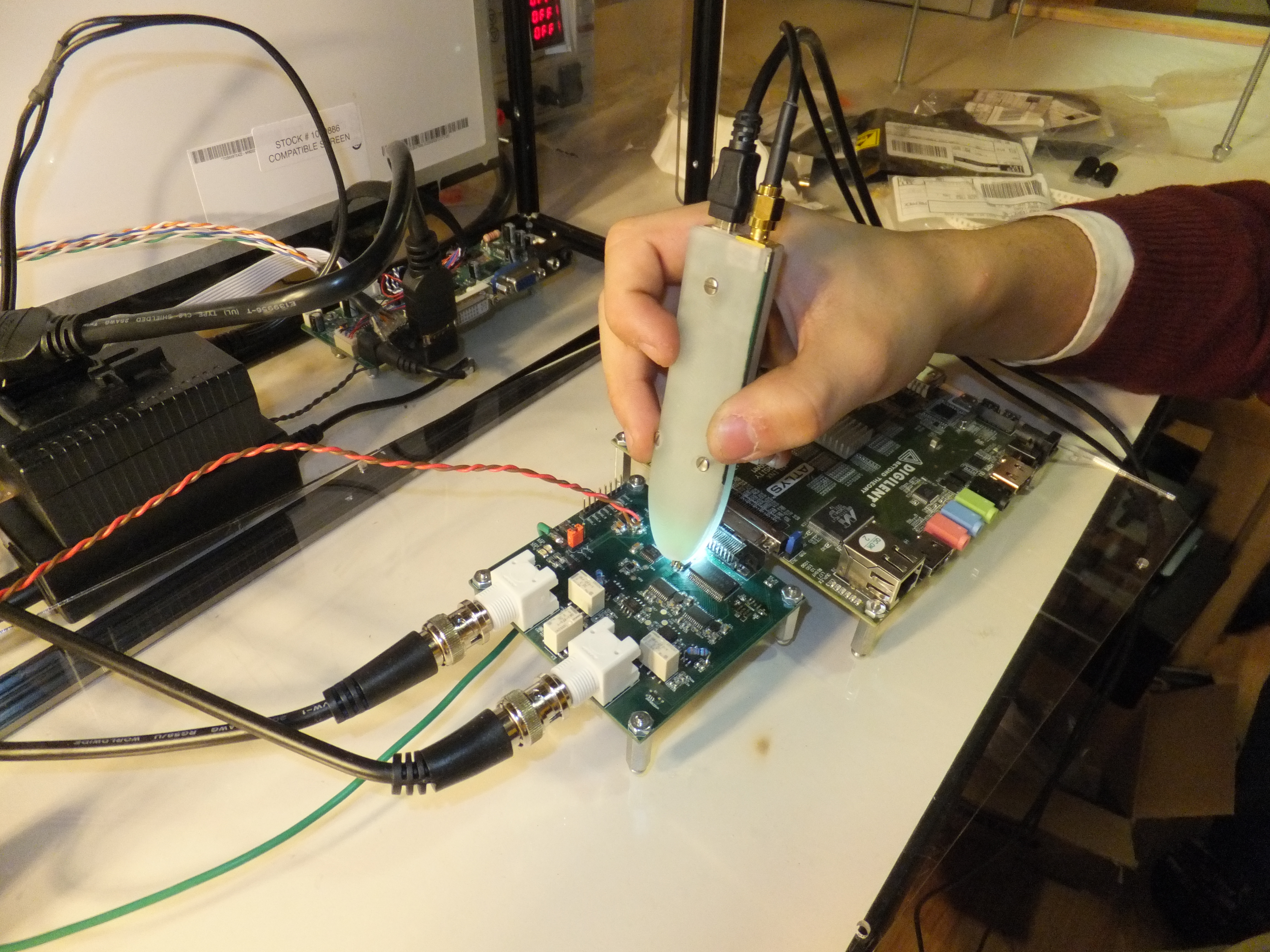
7:00 PM – 9:00 PM: Testing and Measurements
With the board finished, it was time to see what kind of performance we had actually achieved. Ideally, we would use a network analyzer and high frequency signal generator to sweep the input with a sine wave up to a couple GHz and record the response. Of course, that’s a setup that costs at least several thousand dollars (at used item eBay prices), so instead we used my Tektronix CSA803 20GHz sampling oscilloscope to record the step response of the probe to a fast rising edge, and then inferred the upper bandwidth from that measurement. The easiest source of a fast rising edge I had at the time was the scope’s clock output signal, which has a risetime of 1ns. Here’s the risetime of the probe when connected to this signal:
[INSERT PICTURE]
Assuming a first order response (which is an OK assumption here), we can calculate the bandwidth from the risetime of the output of the probe as follows:
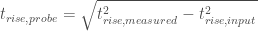

where the measured values for these parameters are


thus,

and

You can read about first order risetimes on this Wikipedia page, and risetimes of cascaded systems are covered later on the same page.
The above measurement was taken with “smoothing” (averaging) enabled on the scope. But what happens when when we disable this and record the same measurement?
[INSERT PICTURE]
What a disaster! There are massive amounts of noise rendering the measurement totally useless for capturing non-repetitive events. While averaging samples over time of a periodic waveform can eliminate the noise, the performance of the probe is not acceptable. At first we panicked because we thought we might have designed the differential amplifier improperly, but if you look closely, you can see that on top of the average level of noise, there are little peaks every once in a while, which are not a characteristic we would except from thermal noise.
The most likely culprit for this sort of problem are noisy power supply rails, especially from the switching converter. Surely enough, not only did the -5V rail had large amounts of noise that would not be acceptable in and of itself, but it also had 300mV peak to peak spikes at the switching transitions.

That MAX1680 thing sure has a noisy output!
Week 2 (February 22, 2014):
Preparations
something something

The PCB Pattern Revised for Week 2
Blah blah blah

Week 2 Revision of the PCB.
hello there
Conclusion and Further Work
The likely reason for this is high dielectric losses in the FR4 PCB material (solution: send out the PCB using Rogers high frequency material) and an impedance mismatch in the 50 ohm trace that connects the final amplifier’s output to the SMA coax connector (solution: use a 4-layer PCB with thin prepreg material so that the trace width required to reach the 50 ohm target impedance is low enough to place on the board; with a 2-layer board the required trace width is too large).
Documentation
Download a PDF schematic here.
Download the EAGLE files here.
Download the gerber files here.
Download the chassis STL files here.

Hi!
Is there possibility to reupload Dropbox files? They are now unavailable. If possible, please drop me the files on email.
Thanks in advance!
Witold
I would buy 2 or 3 bare pcb’s.
Contact me at miwi490 aatt yahoo dddoootttt de, I will order some @ Würth, Ätzwerk or someone else in the EU and can order some more.
I will definitly not take care for lowest pcb-price as it is not very important for me if costs are 10 or 20€ as long as the pcbs are aviablie within 7 workingdays.
Offer for this is closing at 17. june 2015
regards
Michael
Probe Reference Material | Entertaining Hacks
Hi Daniel,
If you’re still reading comments I’d like to say thanks for this article. I used your Gerbers to order a couple of PCBs from Ragworm.eu and built up two probes to use at work. So far so good! I’ll be interested in the revised version when you get round to making it. If you make a batch of the new 4-layer PCBs and want to sell some then let me know.
Cheers
James
Hi Daniel,
following your project, I did start to build a probe with the same case and the THS3202 as differential amp.
https://www.mikrocontroller.net/topic/382504#new
Thank you for your article, great work!
Best regards, 73
Bernhard, DL1BG
Thanks for the article, Daniel. It is a pretty cool project. Would a 32 mil thick pcb work ok with your plastic/printed case parts? I’m thinking that the reduced pcb thickness would achieve the lower stripline impedance without the added expense of going to a 4-layer board.
Thanks,
Eric
I know this is now quite an old project but I am keen to build something like this. The dropbox files have all disappeared. Can they be restored or does anybody have a copy of them or better still any PCBs they are willing sell?
The files are uploaded to github: https://github.com/dkramnik/Eagle-Public
John
the opamp isn`t aviable anymore (NRND) and new parts are aviable since then, (THS3217 and others)
thereis also an actual project at eevblog.com:
https://www.eevblog.com/forum/testgear/gt-1-ghz-diy-differential-probes/?all
Hi,
This is sreehari, in revised PCB you have used IC2,IC3 with 5 pin plz tell what is the part number. this is BOOST regulator? if you don’t mind plz share the pcb file.
Sure, you can find the design files containing the relevant part numbers on my github: https://github.com/dkramnik/Eagle-Public/tree/master/instrumentation-active-probe-makemit-2014
Hi michael,
I am running my won organisation I can not afford to buy the probe, so plz share the gerbers files in pdf format only, based on that I will follow the PCB drawing, it will help me more. Plzzz
you know that the opamp is NRD? And you also know that the whole design is AC-coupled “only”?
I won`t build it again as there are other designs on the net with DC-coupling too. you should study Bernhards design.
Hi xellers,
Thank you.